Bare Metal Flashing of the RP2040
Copyright (C) Bruce MacKinnon, 2025. Contact info at bottom of the page for comments/corrections.
Introduction
I’m working on a radio project that requires the ability to perform a remote flash of the firmware on an RP2040-based board via a low-speed LoRa radio link. The “standard” way to flash an RP2040 board is to use a USB-connected Raspberry Pi Debug Probe (or similar device) attached to a host computer running OpenOCD. That works great on the bench, but I’d like something simpler, more compact, and lower power. That led me to a research project to understand how the SWD-based flashing mechanism on the RP2040 actually works. Is it possible to create a simple device that can drive the SWD pins on an RP2040-based board and update its firmware? Let’s find out.
I’m not going to get into the details of the wireless part of this project in this article - more on that later.
NOTE: Things are slightly different for the RP2350. I will update this document shortly to reflect those differences.
Background: The SWD Interface and Debugging Basics
The RP2040 is flashed using an interface that was originally intended for in-system debugging. In order to understand the flash process, you need to understand the ARM debug mechanism. The next few sections walk through this background. Note that this information may also be useful for other debug purposes unrelated to flashing.
The description of the debug mechanism in the RP2040 datasheet (section 2.4.2.4) is extremely brief. I think the RPi team expects you to either (a) flash using their off-the-shelf debug probe or (b) use the ARM documentation to understand the details of the debug port. I had a hard time piecing this together for myself, but it does work in the end.
The RP2350 datasheet does a slightly better job, but we’re not dealing with that quite yet.
The most important/detailed document is the ARM Debug Interface Architecture Specification ADIv5.0 to ADIv5.2. Per the datasheet, the RP2040 follows the ADIv5.1 specification.
If you already understand SWD/debug you can skip down to the parts about flashing.
SWD Basics
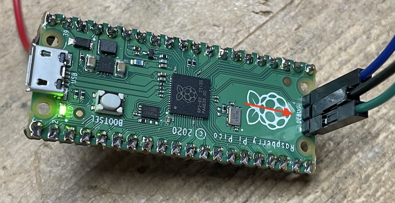
The RP2040 provides a two pin “Serial Wire Debug” (SWD) port. The commercial Pi Pico 1/W boards all break out these two pins into a separate connector that can be attached to a debug probe like the Pi Debug Port, a JLink, or a Segger. The SWD connector is marked in red here:
I’m not going to get into the details of the commercial debug probes since they are described in many other articles. The key thing to understand (which was new to me) is that there is no “magic” involved when driving the SWD port on an RP2040. This two-pin interface works very much like an I2C port and can be driven by any 3.3V-compatible device that can wiggle two GPIO lines in a way that follows the SWD protocol. I’m driving the SWD interface using a second RP2040, but that is not a requirement - any other 3.3V GPIO-capable device could be used to flash an RP2040 board, so long as it follows the SWD protocol rules. I’ve developed my own driver from scratch. I hope this article removes some of the mystery around this process.
Here’s a picture of the setup that I used to build/test my flasher. It’s not that complicated!
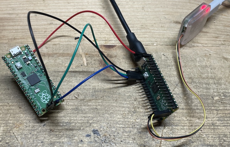
The Pi Pico on the left is the “target” board, i.e. the one being flashed. The Pico on the right is the “source” board where my flashing code is running. My source board is connected to a normal Raspberry Pi Debug Probe and is flashed the normal way.
Debug Hardware
The RP2040 chip contains some special ARM hardware that enables remote debug. This hardware is officially know as a CoreSight compliant Debug Access Port (DAP). External debug/flash systems like the one I am building communicate with the CoreSight hardware via the Serial Wire Debug (SWD) connections.
One thing to understand is that the the CoreSight debug system is almost completely independent of the
Cortex-M0+ processor cores inside of the RP2040. This means that the debug interface runs (and maintains state)
even when the core processor(s) are crashed, halted, or rebooted. This independence is obviously critical for any
low-level debugging capability.
It turns out that the RP2040 flashing process can be carried out over the SWD debug port because of three key enabling features:
- You can read/write arbitrary locations in the RP2040 address space via the SWD port.
- You can command the processor execute arbitrary functions via the SWD port.
- The low-level driver firmware required to erase/write the QSPI flash memory on an RP2040-based board is available in the factory ROM inside of the RP2040 chip.
If you can understand how to use these three features, you can flash the board via SWD.
SWD Physical Interface
As you can see from the previous photo, the two SWD pins of the target board are connected to GPIO pins on the source board. There is also a reference ground pin on the target SWD connector that is tied to the ground on the source board. Unrelated to the flashing process, my target board is being powered from the +5V USB connection on the source board via the red wire (VBUS connection).
There are two pins on the SWD port. They follow normal 3.3V logic:
- The SWCLK pin is always driven by the source. This provides the serial data clock for the target board in the same way what the SCL pin works on an I2C interface. It doesn’t matter too much what frequency this clock is driven at, so long as it falls within the allowable range of the SWD protocol and/or your cables. The RP2040 datasheet suggests a maximum clock rate of 24 MHz. I am using something much slower, around 500 kHz. Importantly, there is no requirement that the clock rate is even constant. I’ve traced the pins on commercial SWD probes and seen all kinds of pauses floating through the protocol exchanges. The important thing is the relationship between the timing on the SWCLK and SWDIO pins - that is critical.
- The SWDIO pin is driven by the source when sending data to the target and is driven by the target when receiving data into the source. Again, very similar to the SDA pin on an I2C interface.
This is a bi-directional serial interface, so all of the complex exchanges of data on the SWD port boil down to a simple process of sending or receiving a bit. Those two processes are explained next.
Sending a Bit to the Target
When the protocol requires the source to send a bit to the target we must make sure that the SWDIO GPIO pin on the source is configured for output. Once that is done, it’s very straight-forward. The code from my driver is the best description of what to do:
    void SWDDriver::writeBit(bool b) {
        // Assert the outbound bit to the slave on the SWDIO data pin
        _setDIO(b);
        // Wait about 1uS for setup.
        _delayPeriod();
        // Raise the SWLCK clock pin. Slave will capture the data on this rising edge.
        _setCLK(true);
        // Wait around 1uS for hold
        _delayPeriod();
        // Lower the SWCLK clock pin.
        _setCLK(false);
    }
Receiving a Bit From the Target
When the protocol requires a bit to be received from the target the GPIO pin used for the SWDIO pin is switched to input mode. The actual receive code from my driver looks like this:
    bool SWDDriver::readBit() {
        // The inbound data is already asserted by the slave on the previous falling
        // clock edge.  Wait about 1uS for setup.
        _delayPeriod();
        // Read the value from the SWDIO data pin
        bool r = _getDIO();
        // Raise the SWCLK clock pin.
        _setCLK(true);
        // Wait about 1uS.
        _delayPeriod();
        // Lower the SWCLK clock pin.
        _setCLK(false);
        return r;
    }
SWD Handshake
There are a few steps that need to be followed to initialize the SWD interface. The details are explained in these documents:
- An IEEE standard document (1149.7) that I don’t have access to.
- A paper called Low Pin-count Debug Interfaces for Multi-device Systems that summarizes the IEEE 1149.7 standard.
- The ARM Debug Interface Architecture Specification ADIv5.0 to ADIv5.2
I will try to avoid repeating everything in these documents. Instead, I outline the precise steps that my (working) flashing code follows. Hopefully I am not doing anything that contradicts the official documentation.
Step 0: Connect the Physical Interface
This is pictured above: connect two GPIO pins from the source board to the SWD pins on the target board, including a ground reference.
Step 1: Initial State
Pull the SWCLK and SWDIO pins low and then send 8 1’s by raising the SWDIO and clocking the SWCLK 8 times.
Step 2: Send Selection Alert
This is a protocol reset message that is needed to get the CoreSight DAP interface into a known state, regardless of what it was doing previously. According to the Low Pin-Count Debug Interface article linked above:
Hence the designers of multi-drop SWD chose an unlikely data sequence approach. The selection message consists of a 128-bit selection alert, followed by a protocol selection command. This selection alert method has been adopted by IEEE 1149.7, and multi-drop SWD has adopted the IEEE 1149.7 protocol selection command, ensuring compatibility between the two protocols.
The source should send 128 bits that look like this:
    0100 1001 1100 1111 1001 0000 0100 0110 1010 1001 1011 0100 1010 0001 0110 0001
    1001 0111 1111 0101 1011 1011 1100 0111 0100 0101 0111 0000 0011 1101 1001 1000
(The spaces above are provided only to make the strings easier to read.)
Step 3a: Send Zeros
4 consecutive 0s are sent to the target.
Step 3b: Send Activation Code
A special activation code is used to enable communication with the ARM CoreSight debug system. The CoreSight code is 0x1a, sent LSB first. The source should send 8 bits that look like this:
0101 1000
(The spaces above are provided only to make the strings easier to read.)
Step 4: Send Line Reset
(The next series of steps is described beginning with section B4.3.4 of the ARM Debug Interface Architecture Specification IHI0031.)
A line reset is sent to the target. A line reset is created by sending 64 consecutive 1s to the target.
Step 5: Send 8 Zeros
8 consecutive 0s are sent to the target.
Step 6: Send a DP Target Select
At this point the protocol starts to follow a standard messaging format that reads/writes 32-bit payloads to specific registers in the target debug interface’s space. The precise mechanics of these read/write transactions are explained below.
This is the part of the handshake sequence were where we decide which of the processor cores we would like to connect to. For an RP2040 the two cores have these addresses:
- Core 0: 0x01002927
- Core 1: 0x11002927
The desired core address needs to be written to the DP SELECT register (0xc). In my testing I always connected to core 0. So 0x01002927 was written to DP register 0xc.
IMPORTANT NOTE: Normally a write transaction would be acknowledged by the target using a 3-bit response code that will be explained below. For this particular step in the protocol (and only this step) the acknowledgement is ignored. Actually, the target doesn’t even drive the acknowledgment phase for this particular step in the transaction because of the multi-drop nature of the SWD bus internal to the RP2040 SOIC.
Step 7: Read the Target’s ID CODE
A read transaction on the DP’s IDCODE (0x0) register is required. The RP2040 will return an IDCODE of 0x0BC12477.
Step 8: Send a Precautionary Abort
A write transaction on the DP’s ABORT (0x0) register is used to make sure there is no work in process.
Step 9: Select AP 0, AP BANK 0, SW-DP Debug Port Bank 0
A write transaction on the DP’s SELECT (0x8) register is used to select AP 0/AP Bank 0/SW-DP Bank 0. I’m a bit unclear on the reason for this step, but it appears to be necessary. Per the ARM documentation the SW-DP port bank defaults to zero anyhow.
Step 10: Send a Power Up of the Debug System
A write transaction on the DP’s CTRL/STAT (0x4) register is used to request that the debug circuits are powered on. The CSYSPWRUPREQ (30), CDBGPWRUPREQ (28), and ORUNDETECT (0) bits are set to 1.
Step 11: Read the CTRL/STAT To Validate Power
A read transaction on the DP’s CTRL/STAT (0x4) register is used to make sure that power on was successful. The CSYSPWRUPACK (31) and CDBGPWRUPACK (29) bits are checked.
I’m not completely sure, but it’s possible that the power-up process is asynchronous. It may be necessary to read these two ACK status bits in a loop. More research is needed, but so far everything seems to come up on the first try.
Step 12: Check AP ID
This step is probably not necessary, but is used to validate the identification of the MEM-AP port in the CoreSight system.
First, AP 0 and AP register bank 0xF are selected by writing a 0x000000F0 to the DP SELECT (0x8) register.
Next, an AP read is performed on address 0xc. This is the AP identification register (0xFC).
Finally, the data from the previous read is retrieved by reading the DP RDBUFF (0xC) register. I am seeing an AP ID of 0x04770031.
Step 13: Leave the AP Bank 0 Selected
First, AP 0 and AP register bank 0x0 are selected by writing a 0x00000000 to the DP SELECT (0x8) register.
Step 14: Configure the AP Transfer Mode
The DP CTRL/STAT (0x0) register is configured to control the AP data access going forward. There are two configurations:
- Auto increment is turned on by writing 0b01 into bits 5:4.
- Word transfer (i.e. 32-bits) is selected by writing 0b010 into bits 2:0.
DP and AP Components
The ARM CoreSight hardware contains two different parts called the Debug Port (DP) and Access Port (AP). The specific roles of these two parts are described in the ARM documentation so I won’t repeat this. Suffice to say, most operations involve the use of registers on both the DP and AP components. Fortunately, the same SWD communication mechanism is used to access registers on both the DP and the AP. Pay close attention to the documentation to make sure you are reading/writing to the right part of the system.
DP/AP Register Write Transaction Sequence
Once the first few “free form” steps of the handshake are complete, all communications between the source/target happen using standardized read and write transactions. These transactions are explained in great detail in the official ARM documentation so I won’t repeat all of that. This section provides a quick summary of the write transaction.
- The source sends an 8-bit write request consisting of:
- A start bit (1)
- The AP/DP select bit. 0 means writing to a DP register, 1 means writing to an AP register.
- The write bit (0)
- A two-bit register address in LSB-forst format. These are the two MSB bits of the four-bit AP/DP register selection. The two LSB bits are always zero.
- A single parity bit (even) across the 8-bit write request.
- A stop bit (0)
- A park bit (1)
- The SWDIO line is released and turned to input mode so that it can be driven by the target.
- A bit is read from the target, but ignored. This is called a turn-around bit.
- A three-bit acknowledgement is read from the target in LSB-first format. A 0b001 code means “success.” Anything else is treated as a failure, although strictly speaking this is not correct since one of the acknowledgment codes (WAIT) means to try again later. I have not implement this because it is not needed in my flashing program.
- The SWDIO line is converted back to output mode so that it can be driven by the source.
- A bit is written by the source, but ignored. This is called a turn-around bit.
- A 32-bit value is written in LSB-first, little-endian format. This is called the data transfer phase.
- A 1 bit parity (even) is written.
Here’s what my driver code looks like so you can see the precise logic:
    int SWDDriver::_write(bool isAP, uint8_t addr, uint32_t data, bool ignoreAck) {

        // The only variable bits are the address and the DP/AP flag
        unsigned int ones = 0;
        if (addr & 0b0100)
            ones++;
        if (addr & 0b1000)
            ones++;
        if (isAP)
            ones++;

        // Start bit
        writeBit(true);
        // 0=DP, 1=AP
        writeBit(isAP);
        // 0=Write
        writeBit(false);
        // Address[3:2] (LSB first)
        writeBit((addr & 0b0100) != 0);
        writeBit((addr & 0b1000) != 0);
        // This system uses even parity, so an extra one should be
        // added only if the rest of the count is odd.
        writeBit((ones % 2) == 1);
        // Stop bit
        writeBit(false);
        // Park bit: drive the DIO high and leave it there
        writeBit(true);

        // Let go of the DIO pin so that the slave can drive it
        _releaseDIO();
        // One cycle turnaround
        readBit();

        // Read three acknowledgement bits (LSB first)
        uint8_t ack = 0;
        if (readBit()) ack |= 1;
        if (readBit()) ack |= 2;
        if (readBit()) ack |= 4;

        // Grab the DIO pin back so that we can drive
        _holdDIO();
        // One cycle turnaround
        writeBit(false);

        // 001 is OK
        if (!ignoreAck) {
            if (ack != 0b001) {
                return -1;
            }
        }

        // Write data, LSB first
        ones = 0;
        for (unsigned int i = 0; i < 32; i++) {
            bool bit = (data & 1) == 1;
            ones += (bit) ? 1 : 0;
            writeBit(bit);
            data = data >> 1;
        }

        // Write parity in order to make the one count even
        writeBit((ones % 2) == 1);

        return 0;
    }
DP/AP Register Read Transaction Sequence
Once the first few “free form” steps of the handshake are complete, all communications between the source/target happen using standardized read and write transactions. These transactions are explained in great detail in the official ARM documentation so I won’t repeat all of that. This section provides a quick summary of the read transaction.
- The source sends an 8-bit read request consisting of:
- A start bit (1)
- The AP/DP select bit. 0 means reading a DP register, 1 means reading an AP register.
- The read bit (1)
- A two-bit register address in LSB-first format. These are the two MSB bits of the four-bit AP/DP register selection. The two LSB bits are always zero.
- A single parity bit (even) across the 8-bit read request.
- A stop bit (0)
- A park bit (1)
- The SWDIO line is released and turned to input mode so that it can be driven by the target.
- A bit is read from the target, but ignored. This is called a turn-around bit.
- A three-bit acknowledgement is read from the target in LSB-first format. A 0b001 code means “success.” Anything else is treated as a failure, although strictly speaking this is not correct - see notes on WAIT above.
- A 32-bit value is read in LSB-first, little-endian format. This is called the data transfer phase.
- A 1 bit parity (even) is read.
- The SWDIO line is converted back to output mode so that it can be driven by the source.
- A bit is written by the source, but ignored. This is called a turn-around bit.
Here’s what my driver code looks like so you can see the precise logic:
    std::expected<uint32_t, int> SWDDriver::_read(bool isAP, uint8_t addr) {

        // Parity calculation. The only variable bits are the address and
        // the DP/AP flag. Start with read flag.
        unsigned int ones = 1;
        if (addr & 0b0100)
            ones++;
        if (addr & 0b1000)
            ones++;
        if (isAP)
            ones++;

        // Start bit
        writeBit(true);
        // 0=DP, 1=AP
        writeBit(isAP);
        // 1=Read
        writeBit(true);
        // Address[3:2] (LSB first)
        writeBit((addr & 0b0100) != 0);
        writeBit((addr & 0b1000) != 0);
        // This system uses even parity, so an extra one should be
        // added only if the rest of the count is odd.
        writeBit((ones % 2) == 1);
        // Stop bit
        writeBit(false);
        // Park bit
        writeBit(true);

        // Release the DIO pin so the slave can drive it
        _releaseDIO();
        // One cycle turnaround
        readBit();

        // Read three acknowledgment bits (LSB first)
        uint8_t ack = 0;
        if (readBit()) ack |= 1;
        if (readBit()) ack |= 2;
        if (readBit()) ack |= 4;

        // 0b001 is OK
        if (ack != 0b001) {
            // TODO: DECIDE HOW TO DEAL WITH THIS
            _holdDIO();
            return std::unexpected(-1);
        }

        // Read data, LSB first
        uint32_t data = 0;
        ones = 0;
        for (unsigned int i = 0; i < 32; i++) {
            bool bit = readBit();
            ones += (bit) ? 1 : 0;
            data = data >> 1;
            data |= (bit) ? 0x80000000 : 0;
        }

        // Read parity
        bool parity = readBit();
        if (ones % 2 == 1 && !parity)
            return std::unexpected(-2);

        // Grab the DIO pin back again so that we can drive it
        _holdDIO();
        // One cycle turnaround
        writeBit(false);

        return data;
    }
Accessing Memory (or Mapped Registers) via SWD
Now the we understand the SWD port, we can get into the process of reading/writing from/to the memory space of the processor.
Unlike some other ARM Cortex parts that you might have used (ex: STM32), it is not possible to write directly into the flash memory of an RP2040 board. This is because there is no on-chip flash on an RP2040. Instead, the flash memory in an RP2040 system is generally contained in an external QSPI flash chip that is mounted onto the board adjacent to the CPU SOIC. The QSPI flash can be mapped into the processor’s memory space and read directly via the RP2040 XIP mechanism, but this doesn’t work for writes. Instead, writes are achieved using a serial protocol that looks more like SPI.
So don’t be confused: when we talk about writing to memory locations in this section, we are not talking about writing to flash memory locations (unfortunately). That said, you still need to be able to read/write the processor’s address space in order to carry out the flashing process that is outlined later.
Reads/writes into the RP2040 address space can be accomplished over the SWD debug port via a part of the CoreSight hardware called the Memory Access Port (MEM-AP).
Reads/writes always happen in 32-bit words on word-aligned address boundaries.
The steps to write are simple:
- Write the address of the word you want to write into the AP TAR (0x4) register. This must be on a word boundary (i.e. two LSBs are zero).
- Write the data you want to write into the AP DRW (0xC) register.
Strictly speaking, the write doesn’t take effect until at least 8 more clock cycles have passed, but that generally happens as part of the next operation so this delay is not noticed.
The steps to read are almost as simple:
- Write the address of the word you want to read into the AP TAR (0x4) register. This must be on a word boundary (i.e. two LSBs are zero).
- “Read” the data you want from the AP DRW (0xC) register. This is a bit tricky because no data is returned by this operation, but instead it is moved into a DP register to be ready for the next step.
- Read the DP RDBUF (0xC) register to get the data.
Accessing Processor Core Registers via SWD
The section above discuss how to read/write data in the processor address space. Unfortunately, the “core registers” of the ARM processor (i.e. PC, LR, R0..R12, etc.) are not memory mapped, so a special mechanism is required to access and manipulate them.
This mechanism involves the use of three registers that are memory mapped, specifically the confusingly-named Debug Core Register Data Register (DCRDR), Debug Core Register Selector Register (DCRSR), and Debug Halting Control and Status Register (DHCSR).
Follow these steps to write to a processor core register:
- Write the data you want to write into the DCRDR (address 0xE000EDF8) using the process in the previous section.
- Write the appropriate selector for the desired core register into the DCRSR (address 0xE000EDF4) using the process in the previous section. This selector will contain a 1 in the bit 16 position signifying a write, and then the register number in bit positions 6:0. For example, writing core register R7 uses a DCRSR selector of 0x00010007.
- Poll (i.e. repeatedly read) the DHCSR (address 0xe000edf0) using the process explained in the previous section until the S_REGRDY bit (bit 16) turns to 1.
Follow these steps to read from a processor core register:
- Write the appropriate selector for the desired core register into the DCRSR (address 0xE000EDF4) using the process in the previous section. This selector will contain a 0 in the bit 16 position signifying a read, and then the register number in bit positions 6:0. For example, reading core register R7 uses a DCRSR selector of 0x00000007.
- Poll (i.e. repeatedly read) the DHCSR (address 0xe000edf0) using the process explained in the previous section until the S_REGRDY bit (bit 16) turns to 1.
- Read the final result from the the DCRDR (address 0xE000EDF8) using the process in the previous section.
As you can tell from the description above, reading/writing processor core registers is an asynchronous process and care must be taken to monitor the S_REGRDY flag to determine when the operation has completed. Reading the DCRDR before the DHCSR indicates that the value is available will result in unpredictable results.
Entering Debug Mode, Halt and Resume via SWD
ARM processors like the RP2040 provide a debug mode that allows us to halt the processor, use the mechanisms described above to read/write memory and/or registers, and restart the processor from an arbitrary location in memory. All of this can be achieved via the SWD port, which is exactly how GDB does its job.
The processor enters debug mode and halts by setting some bits in the DHCSR (address 0xe000edf0) register using a write transaction explained above. Specifically, we need to set:
- Bits 31:16 to 0xA05F. This is a magic key that helps to prevent accidental writing to the DHCSR register.
- Bit 3 must be set to 1 to disable interrupts.
- Bit 2 must be set to 1 to halt.
- Bit 0 must be set to 1 to enter debug mode.
In summary, write 0xA05F000B to address 0xE000EDF0 to halt the processor and enter debug mode.
The processor can be resumed by clearing bits 3, 2, and 0. In other words: write 0xA05F0000 to address 0xE000EDF0 to resume execution.
Resetting into Debug Mode via SWD
Unfortunately, halting a running processor can lead to an indeterminate state since we don’t know exactly what was going on at the time the (asynchronous) halt command was issued. This is solved by resetting the processor directly into debug mode. In this way, the processor doesn’t have a chance to do anything after it is reset - we start from a blank slate.
This behavior is achieved by writing a 1 into bit 0 of the Debug Exception and Monitor Control Register (DEMCR) at address 0xE000EDFC. This bit is called the VC_CORERESET bit and it instructs the processor to enter halt/debug immediately after a reset using the “vector catch” feature.
Once this bit is set, a reset is requested by writing a 1 into bit 2 of the Application Interrupt and Reset Control Register (NVIC.AIRCR) at address 0xE000ED0C. This bit is called the SYSRESETREQ bit and it requests an immediate reset of the processor.
After these steps the processor goes into a clean state and is halted awaiting the instructions needed to accomplish the flashing process.
Calling A Function on the RP2040 Via SWD
As will be seen later, the flashing process involves calling a set of utility functions that are available on the RP2040 chip. This section focuses on the tricky problem of calling a function (i.e. executing code) on the target board via the SWD port. The process described here is exactly the same as what would happen if you used GDB to call a function during a debug session. It took me a while to figure out this part.
The mechanics of this process require some basic understanding of the ARM ABI Procedure Call Standard. The relevant parts of that standard boil down to:
- The PC core register (aka r15) stores the address of the next instruction to be executed. “Calling a function” is as simple as pointing PC to the starting instruction of the function to be called. Normally the PC register would be changed using a branch instruction of some kind (i.e. B, BX, BLX, etc.) but we will use the debugger interface to make this change manually.
- The first four arguments to a function call should be passed in core registers r0, r1, r2, and r3. If you’ve got more than 4 arguments then the stack comes into the picture, but I’ve not looked into this.
- The return address for a function call should be stored in the LR core register (aka r14).
- Function code is aligned on half-word boundaries (i.e. LSB of the function address is 0), but function calls should be made using an address with a LSB of 1 to indicate that the processor should run in “thumb mode.” (Thumb mode is a whole different topic that isn’t covered here.)
The actual steps used to call a function are as follows:
- Use the core register write process described previously to write the first four arguments of the function into core registers r0-r3.
- Write a value of 0x20000080 into the core MSP register so that the function has a valid stack to work with if it needs one. This address is in the RAM address space.
- Write the address of the function you want to call (+1 to indicate thumb mode) into the PC register.
- Read and write the same value back to the Debug Fault Status Register (DFSR) at address 0xE000ED30 to clear any faults from previous calls.
- Remove the halt bit from the DHCSR register to start the processor again. We leave the MASKINT and DEBUGEN flags on, so this step amounts to writing a value of 0xA05F0009 to address 0xE000EDF0.
At this point the process is running again, starting at the first instruction of the function you are trying to call.
Re-Gaining Control After Function Call, Trampoline
The procedure described in the previous section works great, but how do we regain control of the processor in a deterministic way after the function we called completes?
This problem is solved using a clever technique called a “debug trampoline” function. You can think of the trampoline as a wrapper function that does two things:
- Calls the function you wanted to call in the first place.
- On return, immediately halts into debug mode.
If you use this mechanism, you are guaranteed that nothing (besides the function you were trying to call) gets executed.
The RP2040 designers foresaw this requirement and put a debug trampoline function into factory ROM (see later section). The ROM trampoline uses core register r7 to pass the address of the target function into the debug trampoline function. On return from your function, the trampoline uses the ARM BKPT instruction to halt and enter debug mode. So the actual steps to call a function via the SWD interface look more like this:
- Use the core register write process described previously to write the first four arguments of the function into core registers r0-r3.
- Write a value of 0x20000080 into the core MSP register so that the function has a valid stack to work with if it needs one. This address is in the RAM address space.
- Write the address of the function you want to call (+1) into the r7 register.
- Write the address of the ROM debug trampoline function into the PC register. This address is determined using a lookup-table that will be explained later. The two-character identifier for the trampoline function is “DT.”
- Read and write the Debug Fault Status Register (DFSR) at address 0xE000ED30 to clear any faults from previous calls.
- Remove the halt bit from the DHCSR register to start the processor again. We leave the MASKINT and DEBUGEN flags on, so this step amounts to writing a value of 0xA05F0009 to address 0xE000EDF0.
- Poll the DHCSR register until the halt bit (bit 2) turns on, indicating that the BKPT instruction has been hit and the processor is halted again.
You are now at a deterministic breakpoint and ready to call another function.
RP2040 ROM Functions
As mentioned above, there is no flash memory in the RP2040. An external QSPI flash chip provides the necessary non-volatile storage. The code needed to configure a QSPI device to enable reading and writing is quite complicated, so the RP2040 designers placed the QSPI flash driver code into a small (16k) ROM that is masked into the RP2040 chip. This space is known as the “boot ROM.” This ROM also contains other helpful utility functions that are unrelated to the flash memory. Floating point math routines, for example.
In order to expose the ROM utility functions to RP2040 programmers without a bunch of hard-coded addresses in the linker script, each function is assigned a two-character identifier. A lookup table at a known location in ROM provides the mapping between a two-character codes and a pointer to the corresponding ROM function. For example, the code that erases a sector of the flash memory has the code “RE” which maps to 0x00002351 - the starting address of the flash_range_erase() function.
Actually, this lookup table isn’t at a fixed location, but rather a 16-bit pointer to the lookup table is stored at the fixed location 0x00000014 in ROM. This is explained in section 2.8.3 of the RP2040 datasheet. In summary: you can call a function in the RP2040 ROM only after you’ve resolved its address in a lookup table using its two-character code.
Aside: 16-bit Reads Via SWD
Since ROM space is at a premium, 16-bit addresses are used for the boot ROM function lookup table. Since the ROM has 16K of space starting at address 0x00000000, we don’t need a full 32-bit address anyhow.
Pay careful attention when navigating a 16-bit lookup table using the SWD read operation that deals with 32-bit words. I think there is a way to configure the CoreSight MEM-AP device to perform 16-bit reads natively, but I didn’t bother with this. Instead, my driver has a utility function that supports a 16-bit “half-word” read for this purpose. The comments explain the process:
    std::expected<uint16_t, int> SWDDriver::readHalfWordViaAP(uint32_t addr) {

        // Write to the AP TAR register. This is the memory address that we will
        // be reading from. Notice that the read is forced to be word-aligned by
        // masking off the bottom two bits.
        if (const auto r = writeAP(0x4, addr & 0xfffffffc); r != 0) {
            return std::unexpected(r);
        }
        // Read from the AP DRW register (actual data is buffered in the DP and
        // comes in the next step)
        if (const auto r = readAP(0xc); !r.has_value()) {
            return std::unexpected(r.error());
        }
        // Fetch result of previous AP read from the DP READBUF register. Remember,
        // this is a full 32-bit word!
        if (const auto r = readDP(0xc); !r.has_value()) {
            return std::unexpected(r.error());
        } else {
            // For the even half-words (i.e. word boundary) just return the
            // 16 least-significant bits of the word.
            if ((addr & 0x3) == 0)
                return (*r & 0xffff);
            // For the odd half-words return the 16 most significant bits of
            // of the word.
            else
                return (*r >> 16) & 0xffff;
        }
    }
Important Address Ranges in the RP2040
This is documented in detail in the RP2040 datasheet. A quick summary:
- The factory ROM is located at address 0x00000000.
- The QSPI flash memory (when enabled in XIP mode) is located at address 0x10000000. This memory is ready-only.
- The RAM is located at address 0x20000000.
Overview of the Flashing Process
Finally, with all of the SWD/debug background out of the way we can get back to the topic of flashing memory. Here are the key steps:
- The SDK build process is used to create a binary file that is targeted for loading at the flash start address 0x10000000.
- The SWD initialization process is followed to initialize the debug capability on the target board.
- A processor reset is performed with a vector cache to bring the target board into a known/clean state.
- The VTOR register on the target board is set to a RAM location (0x20000000) in preparation for executing functions on the target.
- Memory reads (via SWD) are used to read the ROM function lookup table from the target and determine the addresses of the required boot ROM functions that will be used during the flashing process.
- A ROM utility function (IF, connect_internal_flash()) is called on the target to reset the QSPI flash chip.
- A ROM utility function (EX, flash_exit_xip()) is called to put the flash into serial write mode.
- A ROM utility function (RE, flash_range_erase()) is called to erase the flash memory.
- A ROM utility function (FC, flash_flush_cache()) is called to flush any internal caching related to the flash memory system.
- For each 4K page from the binary to be stored in flash:
- The page is written into a RAM workarea on the target board starting at address 0x20000100. This is done using 1024 32-bit word writes.
- A ROM utility function (RP, flash_range_program()) is called on the target board that copies 4K of data from RAM to flash.
- A ROM utility function (FC, flash_flush_cache()) is called to flush any internal caching.
- A ROM utility function (CX, flash_enter_cmd_xip()) is called that re-enables XIP and allow the flash memory to be read normally.
- For each 4K page from the binary to be stored in flash:
- The page is written into a RAM workarea on the target board starting at address 0x20000100. This is done using 1024 32-bit word writes.
- A comparison is performed between what is in the RAM workarea and what is stored in flash to validate the flashing process. This is done using 1024 32-bit word compares.
- Debug mode is exited on the target board.
- The target board is reset again, thus beginning the normal boot process and the execution of the newly flashed program.
Notes on Build Process/Binaries
The normal SDK build process can be used to create a binary file that can be flashed onto an RP2040 board. The output of that build process is generally an .ELF file. One final step is needed to convert the .ELF to a raw .BIN file that is suitable for flashing:
arm-none-eabi-objcopy -O binary main.elf main.bin
How to Perform a Partial Flash of the User Application
(Work in process, future)
References
For RP2040:
- RP2040 Datasheet
- ARM Debug Interface Architecture Specification ADIv5.0 to ADIv5.2
- Low Pin-count Debug Interfaces for Multi-device Systems
For RP2350: