IBM 1620 - Signs of Life
Everything in a processor is driven by a master clock. To find the heart of the IBM 1620, you need to find the source of this clock. After some hunting through the Model 1F ALDs, I found a page named CLOCK OSC + CONTROL (01.10.05.01) that looked promising. The TAF card at gate B, panel 1, row A, column 15 labeled “OSC” is noteworthy because it has no inputs.
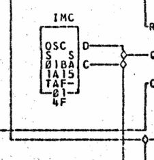
It doesn’t look like much in the middle of ~400 pages of ALD diagrams, but this card is the source of the Nile. It contains a crystal oscillator that produces a 1 MHz clock pulse. Everything else in the processor is driven, in one way or another, by pins C/D of this TAF card.
Simulation at the SMS Card Level
This important TAF card is just one of 100’s of cards that make up an IBM 1620. A pretty detailed understanding of SMS technology will be required.
The IBM Standard Modular System (SMS) technology is interesting and is well documented in other places. I would particularly encourage you to check out Ken Shirriff’s oustanding website and SMS database for more information. The key elements:
- The 1620 and other IBM machines of the era were assembled using a modular card system. Logic designers chose from a library of existing modular cards, or invented new cards to realize their circuits.
- These cards used a standard form factor and plugged into the computer frame using a 16 pin connector.
- There are about 80 unique SMS cards used in the core 1620 processor.
- Thankfully, we have schematic diagrams for all of the SMS cards.
In order to simulate the full computer we need an accurate model of the behavior of each card. There are some excellent instruction-set emulators available for the 1620, but from what I can tell, nobody has attempted to model the electronic behavior of the system. (If you’ve done this already please drop me a line!)
I started with NGSPICE because I’m familiar with it, it is a widely used circuit simulator, and it will do a good job of accurately modeling the SMS cards down to the transistor level. NGSPICE is an evolved flavor of the classic SPICE simulator created at UC Berkeley in the 1970s.
IMPORTANT: The default PNP transistor models in NGSPICE are based on modern silicon devices. I’ve been using a SPICE transistor model file that more closely simulates a germanium transistor, but this is far from accurate at this time. In particular, the early transistors used in the 1620 undoubtedly had some relatively huge parasitic capacitances that impacted performance. I’ve not tackled this problem yet so many of the simulations present an unrealistically “sharp” view of the analog waveforms. I will do some work on this facet of the model later.
And don’t worry - I’m not planning to model the entire computer in SPICE! That model would be prohibitively large, and such analog detail is not really required. However, SPICE models are a great way to fully understand the relevant SMS cards and to get the key sections of the ALD logic diagrams nailed down. The full machine simulation will likely happen using Verilog. Verilog will support a more logical (digital) simulation and will not attempt to model all of the analog nuances of the circuit.
Looking at the TAF Card
I’ve started my simulation journey with the TAF oscillator card. You normally think of a computer as a digital circuit, but this card is all analog. Anyone who works on RF/radio circuits will find this circuit very familiar. It’s an amplifier with a 1 MHz crystal in the feedback path. The bottom part of the circuit contains a tuned tank circuit made up of a 100 μH inductor and a 150 pF capacitor. 1/(2 * PI * sqrt(LC)) = around 1 MHz.
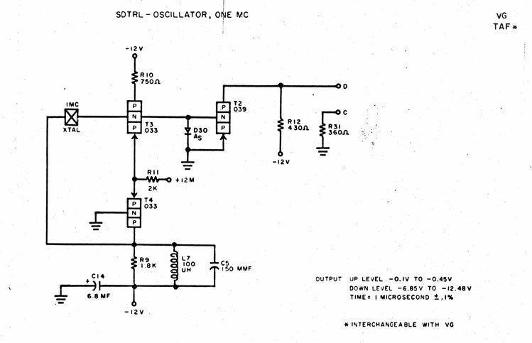
As an aside, IBMs circuit diagrams use a few different (and confusing) notations for capacitors. For this circuit we can be confident that C14 6.8 MF is being stated in microfarads, not millifards. And we know from the above resonance calculation that C5 150 MMF is stated in micro-micro Farads, better known as picofarads.
I modeled this circuit in NGSPICE. The SPICE file for this card is included below so you can get an idea of what it looks like. (For all other cards please reference the official IBM 1620 Github site.)
To make things easier, I’ve maintained IBM’s component numbers and have named the inputs/outputs using the same pin letters as the real SMS card uses.
* TAF - SDTRL - OSCILLATOR, ONE MC
* https://static.righto.com/sms/TAF.html
* SPICE model of IBM SMS logic card
* Bruce MacKinnon 7-June-2024

.SUBCKT SMS_CARD_TAF a b c d e f g h j k l m n p q r

* Standard aliases for power pins
Rx0 vp12 n 0
Rx1 vn12 m 0
r10 vn12 t3_c 750
* Pull in my approximation of a crystal filter
x1 t3_b t4_c CRYSTAL_1MC
* PNP transistor
* Qx nc nb ne mname
q3 t3_c t3_b t4_e pnp033
* Clamp diode
d30 t3_b 0 diodeAS
* Final buffer transistor
q2 d t3_b 0 pnp106
r12 d vn12 430
r31 c 0 360
r11 vp12 t4_e 2k
q4 t4_c 0 t4_e pnp033
* Tuned tank circuit (~1.2 MHz)
r9 t4_c vn12 1.8k
l7 t4_c vn12 100u
c5 t4_c vn12 150p
* Big supply bypass
c14 vn12 0 6.8u

.ENDS
That’s it - there’s really not much on these cards. If you hook up the ground/power, tie pins C and D together like the ALD says, and run the SPICE simulation you get this incredible trace on pin D:
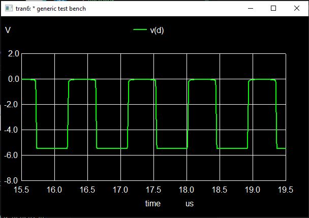
It is alive! It’s hard to believe. You get a nice 1μS clock signal, just like the real 1620.
Putting Together the Clock Drive Circuit
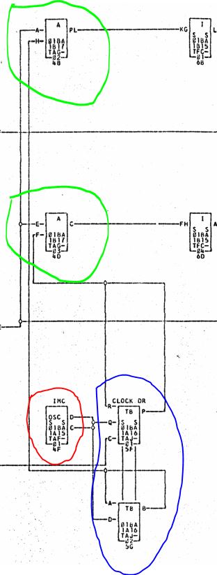
Zooming out on the ALD you see a few more parts that are needed to create the full clock drive circuit.
The red circled area is the TAF that we’ve got already. The blue marked area is a TAJ card which implements a binary flip-flop trigger (more on that important card later). The two TAG cards in green are NAND gates to buffer and to allow the clock to be turned off in certain conditions.
After modeling the TAJ card and hooking it up to the TAF clock I got this:
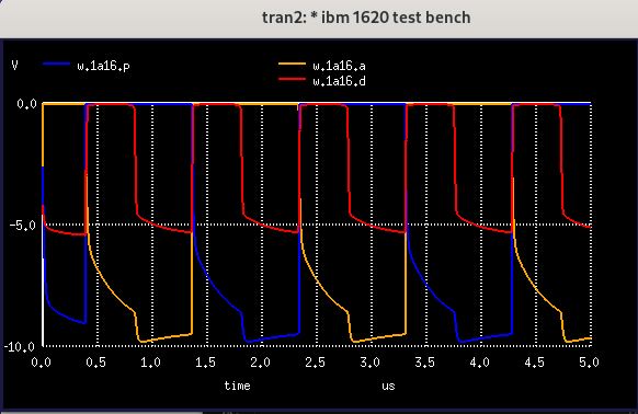
What you’re seeing here is the output of the TAF oscillator in red, and the output of the two sides of the bistable flip-flop circuit (TAJ card) in blue and yellow respectively. There are a few interesting things to note here:
- At this point in the development, my SPICE models were being stitched together from the result of ALD scans. The wire labels that are shown on the top of the image (EX: w.1a16.p) represent the actual card/pin locations in the 1620 frame. Actually, the gate letter is missing, so more work is needed on this.
- The traces look “more analog than digital.” Now that the TAJ card is loading the oscillator output, the traces start to look more like they would in the real world. The curved behavior in the blue and yellow traces results from the fact that the TAJ card contains capacitors. These signals will get “cleaned up” a bit by the next stage of the circuit.
- Unlike modern processors, the IBM CTRL/SDTRL technology used in the 1620 uses a voltage around -0.5V to represent a logical “1” and a voltage around -12V to represent a logical “0.” This will take some getting used to. (I’ll get into the PNP logic circuit in a future post.)
- The blue and yellow traces alternate on each cycle. The TAJ card is a divide-by-two flip-flop that produces even and odd clock drives.
After the TAG card was modeled and the A/1/B17 card was virtually “plugged in,” you can see the cleaned up clock drives that are sent to the rest of the machine. Clock Drive B is on the top and Clock Drive A is on the bottom:
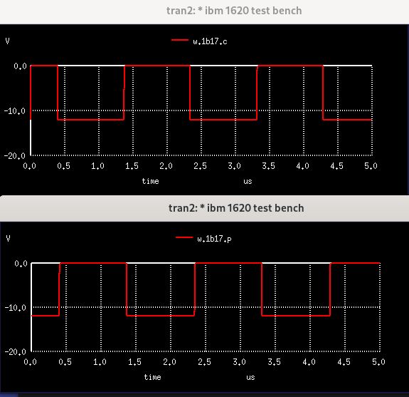
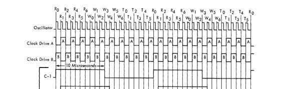
Which matches what the CE manual says we should see:
This gives you a general idea of how the machine is put together. The simulation concept seems to be working and I’m starting to get slighly confident that this whole idea is going to work. :-)