IBM 1620 - Digital Clocks
In my last post I described a SPICE model of the 1620 clock generation circuit. SPICE models are nice because they account for the electrical behavior of every component in the machine - right down to the last resistor. Given that my goal is to run software, an analog simulation is unnecessarily detailed. A digital abstraction should suit our needs.
SMS Card in Verilog
This is a gross simplification, but this particular digital computer considers voltages above -0.6V to be logical ones and voltages below -10V to be logical zeros. Under this simplification, all of the complex analog currents flowing through the transistors, diodes, resistors, and capacitors on the SMS cards can be boiled down to Boolean logic.
This is where Verilog comes into the picture. Verilog is a popular hardware description language that allows a designer to express a detailed specification of a digital circuit. The Verilog ecosystem includes open-source compilers, simulators, and synthesizers that we can leverage for this project. I use Icarus Verilog written by Steve Icarus.
The digital abstraction of an analog circuit has the advantage of being much easier to encode and much faster to simulate. My guess is that a state-of-the-art Verilog simulator will run at about the same speed as a 1959 computer, but we’ll see!
Here’s the Verilog for the TAF card to give you a sense of the model:
module  SMS_CARD_TAF(output c, output d);
    reg clk = 0;
    assign d = clk; assign c = clk;
    always begin
        // Constant clock
        // We are assuming a timestep of 1ns.  This gives a 1 MHz frequency with
        // a 20% duty cycle. There's nothing special about 20% - it's arbitrary.
        #800 clk = 1;
        #200 clk = 0;
    end
endmodule
Compare that to the SPICE model on this page to see how much simpler the digital model is. It is my hope that the behavior of the digital parts of the IBM 1620 can all be expressed in Verilog form. There are a few nuances of the way CTRL/SDTRL logic works that may get in the way, but we’ll see how this goes.
A Verilog Model of Multiple SMS Cards
I developed a translation program that converts my digitized ALD format to Verilog. The translated scan of part of the clock generation ALD page (01.10.05.1) looks like this:
  wire W_HIZ0_A;
  wire W_9991_A;
  wire W_1A16_A;
  wire W_1A16_D;
  wire W_1A16_P;
  wire W_1B17_P;
  wire W_1B17_C;
  // Card HIZ at location HIZ0 - High Impedance
  SMS_CARD_HIZ X_HIZ0(.a(W_HIZ0_A));
  // Card ONE at location 9991 - Logical 1
  SMS_CARD_ONE X_9991(.a(W_9991_A));
  // Card TAJ at location 1A16 - SDTRL-Trigger, Binary
  SMS_CARD_TAJ X_1A16(.q(W_1A16_D), .a(W_1A16_A), .c(W_HIZ0_A), .d(W_1A16_D), .b(W_1A16_A), .p(W_1A16_P), .r(W_1A16_P));
  // Card TAF at location 1A15 - SDTRL-Oscillator, One MC
  SMS_CARD_TAF X_1A15(.d(W_1A16_D), .c(W_1A16_D));
  // Card TAG at location 1B17 - SDTRL-2Way Inverter
  SMS_CARD_TAG X_1B17(.a(W_9991_A), .h(W_1A16_A), .e(W_9991_A), .f(W_1A16_P), .p(W_1B17_P), .c(W_1B17_C));
Don’t worry, I’m not typing that part by hand. The digitized ALD is the master representation and what is shown above is a machine-generated “wire-up” of the SMS-level Verilog models.
When I compile that Verilog, along with my Verilog models of the TAF, TAJ, and TAG cards, run a Verilog simulator, and display the result in GTKWave, I see this output:
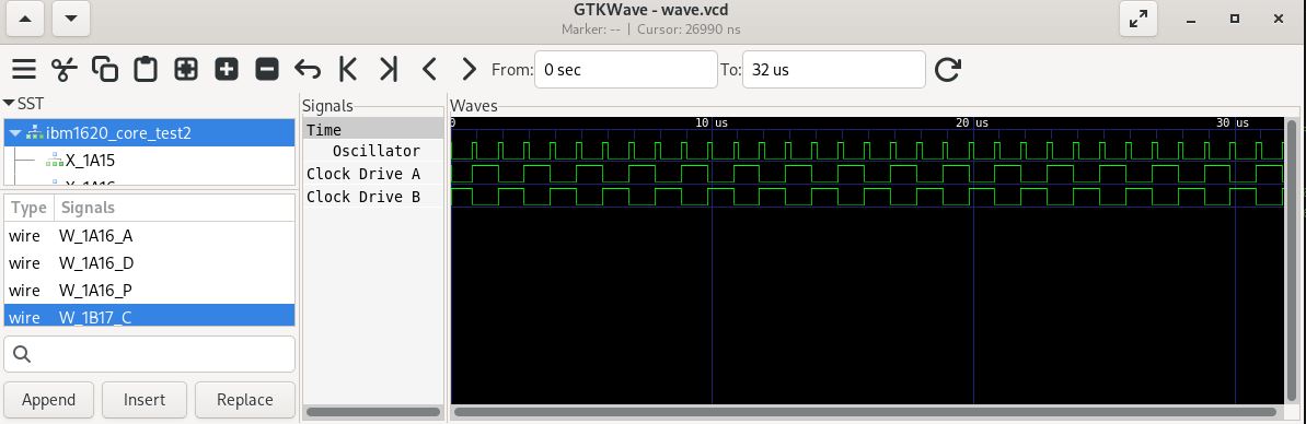
As a reminder, here’s the clock signal picture provided in the CE manual. The first three lines match perfectly!
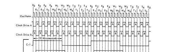
I think we’re still on the right track. I’m now working on the more detailed timing phases, like “C-1” shown in the CE manual above.