IBM 1620 - Automated Logic Diagrams, Early EDA
This project would not have been possible without access to the actual schematics of the IBM 1620. A huge thanks goes to Dave Babcock who has loaned me his set of original model 1F system diagrams, complete with the cool 11”x17” binders. Dave led the Computer History Museum’s IBM 1620 restoration project, the museum’s IBM 1620 Jr. project, the spinoff Cadetwriter project and wrote the SPS1620 assembler. Some of his amazing work can be found here.
When I looked at the 1620 schematics for the first time, I immediately wondered how they were created. The volume and complexity of these diagrams is impressive, particularly when you imagine a world before high-resolution graphic displays, mice, and laser printers. Clearly, the design team was working with some advanced tools.
I had the pleasure of working as a VLSI designer on a mainframe development team at the IBM Poughkeepsie lab in the early 1990’s. It was obvious at that time - and is still today - that electronics designers are only as productive as the their software tools allow. Modern-day tools like Cadence, Synopsys, KiCad, Altium, and ANSYS are the bread and butter of electronics design.
An investigation of the design tools used by the 1620 team provides some interesting insight.
Engineering Design Automation in 1959
A computer of even modest complexity requires the integration of thousands of small components. There are more “moving parts” in a computer than any person can reasonably keep in their head. To manage the daunting complexity of designing a next-generation computer, an engineering team relies on the previous-generation computer. So-called engineering design automation tools (EDA) are a way of life for all electronics designers. Fortunately for us, the invention of EDA systems and the creation of the 1620 were coincident.
An article on the Computer History Museum Website credits IBM, and specifically the work going on at the Poughkeepsie labs, with the invention of EDA. As this article points out: “… IBM pioneered EDA in the late 1950s with documentation of the 700 series of computers.”
The IBM Transistor Component Circuits Manual from 1959 (hosted on the excellent ibm-1401.info website) contains this paragraph (pg 13) that confirms that EDA tools were in common use at IBM during the 1620 era:
Automation of design was initiated because of the large volume of paper work required in the design and manufacturing of new data processing equipment. This program uses an IBM 704 or 705 to provide a fast and accurate method of preparing and up-dating the information necessary to support engineering and manufacturing. Automation of design eliminates the slow and costly manual drafting procedures previously used.
IBM’s Early Computers (by Bashe, Johnson, Palmer and Pugh - MIT Press, 1986) also mentions the significance of design automation in their chapter covering the advent of transistor technology:
Finding ways to provide computer assistance in all aspects of research, development, and manufacturing had been a goal of the Poughkeepsie engineers for some time. The pressing need to reduce paperwork associated with the design and test of large systems had become evident during the design of the 701 and 702 computers. To help control this problem, information about the characteristics and form of standard circuit elements was stored in the computer, and methods were developed to enable the computer to print out logic block diagrams. Engineering changes were facilitated by the records kept in the computer, and the introduction of new errors was reduced. It was the beginning of design automation in IBM; the term itself came into common use at this time.
The primary EDA technology that both of these books is referencing was called the “Design Mechanization System.” This revolutionary system produced, among other things, the Automated Logic Diagrams (ALDs). It’s ironic that in both of the quotes above the elimination of paperwork is highlighted, yet the only representation of the 1620 circuit we have left is in giant binders spanning nearly 400 pages of paper ALD diagrams. Thank God for paper records!
There’s another interesting IBM Research article entitled EDA In IBM: Past, Present, and Future which provides a lot of detail of IBM’s innovations in the design automation space. Unfortunately, the author’s definition of “past” starts somewhere in the S/370 era (late 1970’s) so it completely misses the innovations that enabled the 1620 design (not to mention the 1401, 7090, and S/360). I used many of the tools described in this paper while working at the Poughkeepsie lab in the early 90’s and can attest to the level of sophistication that the EDA team at IBM had built up over the years.
Automated Logic Diagrams (ALDs)
Thanks to Dave, I have access to a set of ALDs for a 1620 model 1F. The ALDs are a subset of the contents of a three-volume set of IBM 1620 System Diagram binders that were used by the Customer Engineers (CEs) who installed and serviced the machines. (As an aside, the fact that this level of detail was sent into the field tells you something about the sophistication of the IBM CEs of that era. Supporting these machines was more than just swapping cards and rebooting until an error code cleared.)
Here’s what Dave’s binders look like:
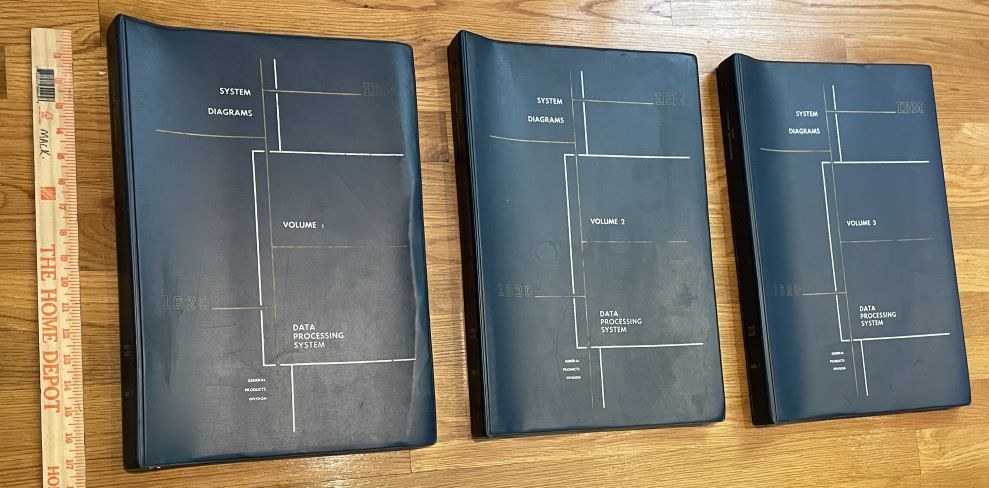
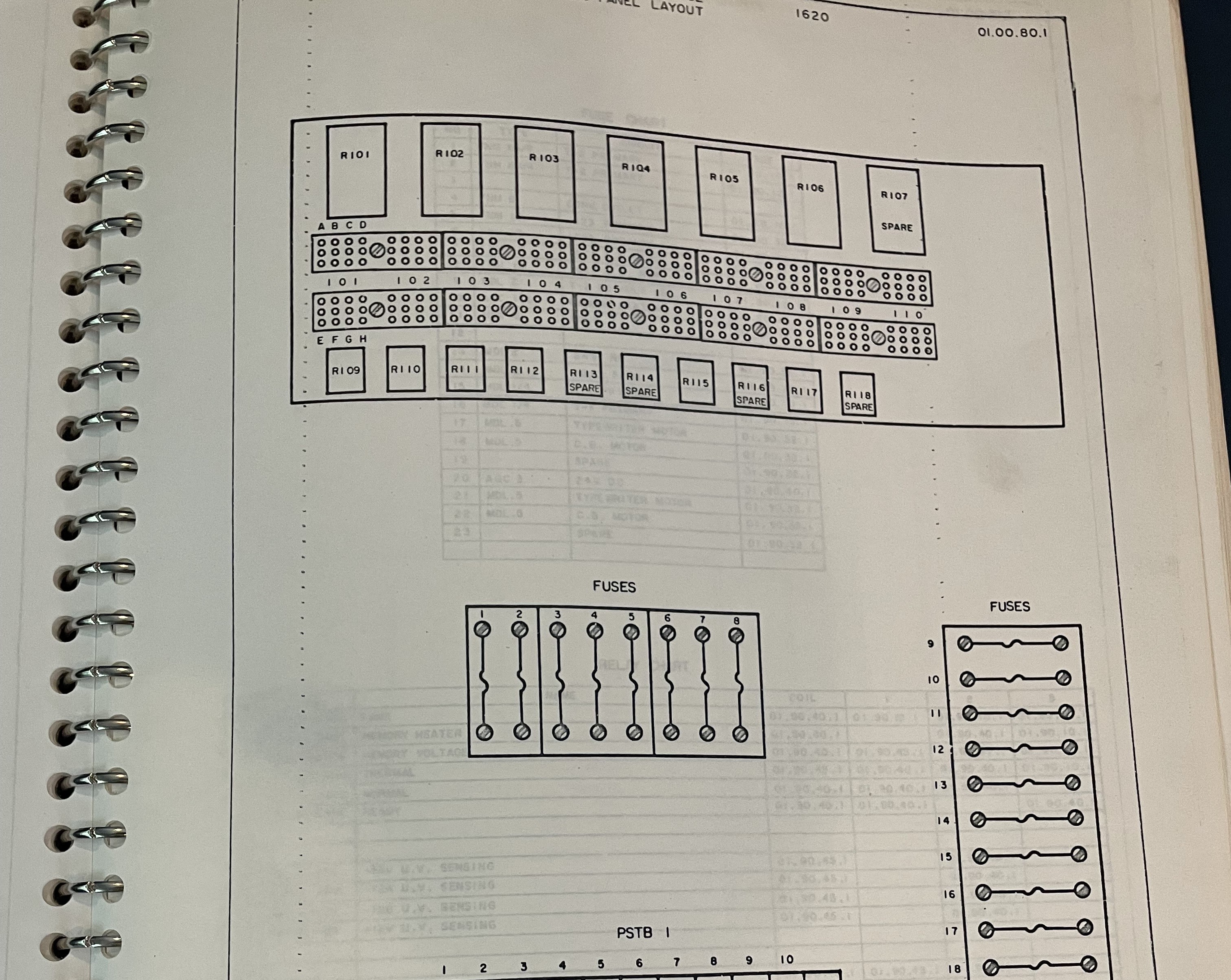
Each book contains large 11x17 inch pages that provide the low-level technical detail of the machine. Strictly speaking, not all of the pages in these books are ALDs. Some of diagrams look more like traditional engineering schematics. For example, a mundane diagram of the 1620 fuse panel is included on page 01.00.80.1:
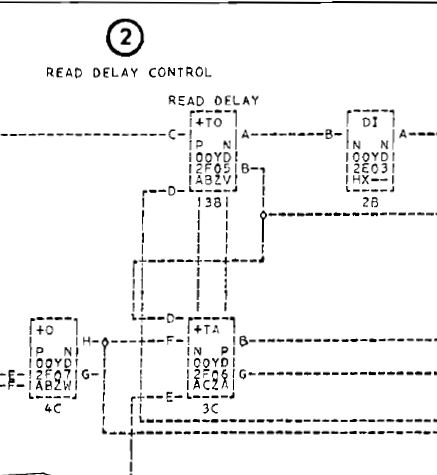
Things get interesting from a software simulation standpoint in the section of the System Diagram books that contains the complete ALD of the referenced machine. Here’s an example of an ALD page:
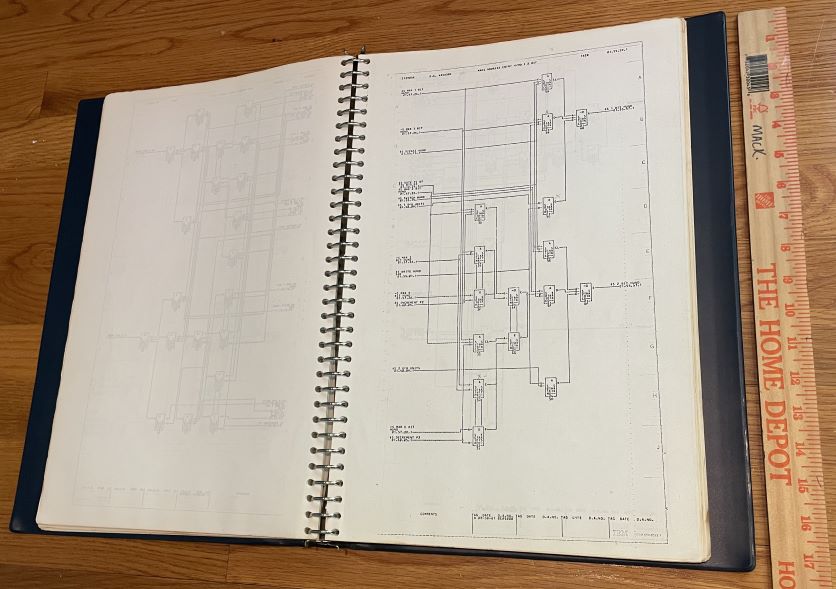
The ALD concept was developed in close association with the SMS card technology used in the 1620, 1401, and other machines of that vintage. These diagrams follow a distinctive style that consists of a 5x9 grid of logic blocks, a network of interconnect wires, and text cross-references to indicate where wires connect to other pages in the ALD. Importantly, the blocks on the ALD pages don’t correspond directly to SMS cards, but instead depict logical subsets of the cards called “circuits.” For example, if a particular SMS card contained three logical NAND circuits, the use of this single card would appear as three distinct ALD blocks, not necessarily adjacent to each other. In this way, the designers could express the logical flow of a computer design in a way that was slightly abstracted from the electrical schematic or mechanical organization. Adjacent blocks on an ALD could represent cards on completely different panels.
The interpretation of these diagrams takes some getting used to. There are two good sources of information:
The IBM Customer Engineering Transistor Component Circuits manual, here linked from the 1401-info website, contains a brief section starting on page 13 that talks about the ALD notation. The 1620-oriented reader should not take these pages too literally since it is clear that the ALD notation evolved over time. The 1401 ALDs appear to have been created using a slightly later version of the software than the 1620 used.
More background is provided in an article by Kloomok/Case/Graff published in the 1958 Proceedings of the American Federation of Information Processing Societies (AFIPS, now absorbed by the IEEE). Key points of the design process:
- Engineers first “sketched” their logical designs on special velum forms that were pre-printed with the characteristic 5x9 grid. The article’s use of the term “sketch” is a bit misleading, since the forms enforced a grid structure down to the level of individual characters. This was a lot more than a casual sketch on the back of a cocktail napkin.
- The hand-written design forms were delivered to a team of clerks affectionately called “transcribers” for key punching. The article highlights the fact that these forms were structured such that “no knowledge of circuit logic or convention is required” to do this data entry job. The claim is made that a transcriber clerk could be trained in “about one week.” Pretty impressive.
- Key-punched design pages were written to the so-called “Master Tape,” which was a sort of database representation of the machine design.
- The Master Tape was then used to print an automated representation of the design diagrams which were returned to the engineering team for review and modification.
- A rigorous change-control workflow was used to manage ECs. This involved another set of forms and another set of records added to the Master Tape. Through this method, every step in a design’s evolution could be tracked.
- In the end, the Master Tape could be sent to manufacturing where it would drive various automated assembly processes.
From the perspective of the reverse-engineering project, one of the most interesting parts of this article is the section entitled: Print Program. The authors describe how the ALD designs encoded on the Master Tapes were converted back into the paper diagram form that we find in our binders today. In the modern day we might call this process “ASCII art.” Key points:
- An IBM 717 printer was used, which was part of of the 705 accounting system. More below.
- Blocks are 6x7 characters. The location of each block on the page is fixed, as is the the location of the characters within the block.
- The total page is 120x186 characters. This an aspect ratio was chosen to fit on 11”x17” B-size ledger paper. Remember: the computers/printers being used here were originally designed for accounting purposes.
- The wiring lines on the diagrams were automatically routed by the software, based on the engineer’s specification of starting and ending locations. This is very impressive.
- The paper describes the creation of an in-memory representation of the entire 120x186 character page (22,320 characters) during the printing process. The creation of this “frame buffer” of sorts required an average of 45 seconds of computer time on the 705. To put this in perspective, the base 1620 core memory could store 20,000 decimal digits. This gives a sense of how the early EDA tools were pushing the boundaries of technology.
- Each page required 75 seconds to print at 150 lines/minute.
Here’s a close-up view of one the the 1620 ALDs:
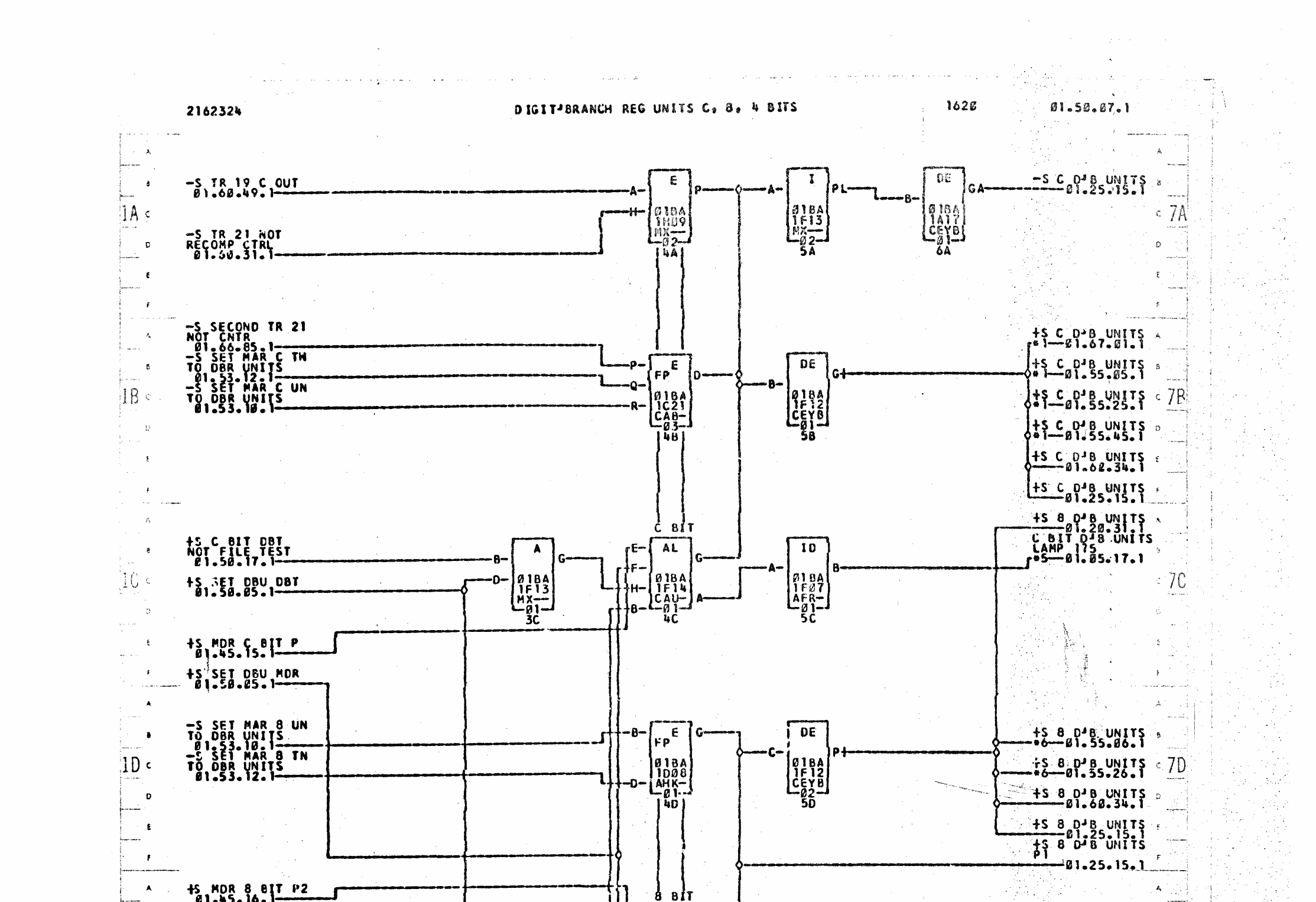
The text inside of each block describes the physical location of the circuit (i.e frame/gate/panel/row/column), the type of SMS card used (ex: MX–), the circuit number, and the grid location on the page (ex: 4C). The letters around the perimeter of the block correspond to the pin letters of the SMS cards.
When wires cross using this symbol: ┼ then they are not electrically connected. When wires cross using a diamond symbol then they are electrically connected.
(There’s another article about the DMS here. from a 1962 conference that covers much of the same ground.)
Notes on the 717 Printer
The Kloomok/Case/Graff article specifically mentions the 717 printer. I’m not able to find much information about that device. According to one document I found, the 717 was a variant of the 716 that is more widely documented.
Paul Kimpel, creator of the retro 1620 and numerous other interesting emulators checked into this and determined that the 717 was used with the 702 and 702 systems, both of which were derivatives of the print mechanism used in the IBM 407 accounting machine. The 407-class printers had interchangeable print wheels, and there were several standard sets, e.g., a “scientific” set for FORTRAN. Per Paul, there were a number of custom wheel-sets for specific applications. It is clear that one of those specialized wheels was used for printing ALDs.
According to an IBM article, the 717 “ALD wheel” (for lack of knowing its official name) contained 48 characters: the 26 upper-case letters, the numbers 0-9, and twelve “special characters.” From what I can tell from Dave’s ALDs, those special characters were the period, plus, minus, pound/hash, and the characters needed to produce the distinctive box/wiring diagrams (horizontal line, vertical line, top left corner, top right corner, bottom left corner, bottom right corner, cross, and diamond). This finally explains the use of the odd “bottom right corner” character in many of the 1620 page names and signal names seen in the ALDs. For example, look at the title line of the diagram above: DIGIT┘BRANCH REG UNITS C, B, 4 BITS. Or page 01.10.12.1: TIMING SAMPLE GENERATION A┘B. That strange mark was obviously being displayed in place of the slash character which wasn’t available on the modified 717 printer. (NOTE: That bottom-right-corner symbol is Unicode x2518 if you need to type it.)
You can see that the example ALD rendering in the Transistor Component Circuits guide was printed on using a less sophisticated print wheel since the wiring looks like more ASCII art as we would recognize it today.
The wiring in the 1620 ALDs has a much cleaner look:
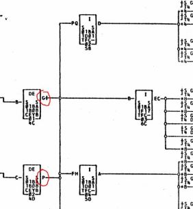
The 717 print wheel used in the 1620 ALD apparently extended the box drawing elements to the extremes of the character impression area to allow lines to link continuously. Not bad for a re-purposed accounting machine!
Points Relevant to ALD Scanning
The Kloomok/Case/Graff article mentions something that is highly relevant to our project: “… based on experience to date … 2.5 to 3 man-hours (are required) to transcribe and key-punch a logic page entry.” I think the authors were highlighting this as a positive aspect of IBM’s capability - presumably in contrast to the many days that would have been required to maintain and update such a diagram on a drafting table using a pencil and T-square. But clearly, I don’t have the time, resources, or patience to re-key all of these diagrams. Automated scanning is critical to success. (NOTE: If anyone has access to a 1620 Master Tape please reach out! :-))
The same article concludes with an appendix that talks about the value of a so-called “Checking Program” that was used to identify design errors in advance of manufacturing. I have transcribed several of their rules here because they will apply to any modern scanning system I create. 60 years later, the same rules apply:
- Two lines with the same name can’t leave from different blocks.
- The set of available SMS cards is known in advance and can be checked.
- The legal set of pin names for each block type (i.e. card/circuit) is known in advance and can be checked.
- The SMS cards can only be chained in certain combinations.
- Lines and/or signal names that don’t connect to anything can be detected.
- Lines that connect to non-existent blocks or signal names can be detected.
- Inconsistencies between ALD pages and machine plugging charts can be detected.
- Multiple uses of the same circuit on the same SMS card can be detected.
There are some important nuances of the 1620 ALD format which need to be understood to properly simulate the machine. I will cover these in more detail in a future post.
The background in this post provides important perspective that makes the scanning process seem feasible: the 1620 ALD diagrams were machine-generated according to a highly rigid format. We’re not trying to interpret handwriting or free-form diagrams here. As long as we can deal with the “noise” associated with the printing/photocopying technology, a systematic interpretation of a 120x186 matrix of characters printed on a 11x17 inch page using a 48-character monospace font should be doable using modern technology. After reading about the history of EDA at IBM, I am very confident that the development team working at the Poughkeepsie Lab in the late 1950’s could have solved this problem in a few weeks. :-)
Ever Onward IBM!