IBM 1620 - ALD Nuances, Part 1
At first glance, the ALDs provide a simplistic wiring diagram between lettered pins on logic blocks. However, there are a few nuances that are worth studying because they are critical to a correct simulation.
(Please make sure you have read the last post first to get some basic orientation to the ALDs.)
Dot AND
It is common to see a single output pin driving the input pins of several different other logic blocks. This one-to-many connection is the traditional “fan out” concept that is present in almost all digital logic designs.
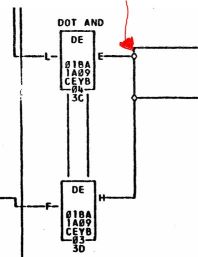
However, notice that in the picture below (1F ALD page 01.10.15.1) two output pins are connected together, and then go off sheet to drive five other places. This case requires some research.
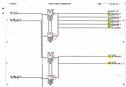
The “DOT AND” note above the blocks provides a hint that something unusual is happening, but keep in mind that the text above a block is for human reference only and cannot be relied upon to describe electrical behavior. In fact, here an example of the same situation without any special notation:
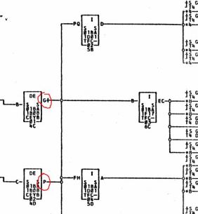
This case is only identified by the fact that the outputs of two different circuits are connected to the same wire.
(Side Note: In the picture above there is a mysterious “+” immediately to the right of the G on one of the two CEYB blocks. I’ve seen this in other places in the ALDs and have not been able to figure out whether it is significant, is a typo, or is a glitch in the ALD software. There is no mention of this notation in the ALD articles that I’ve read. I would welcome any experts to comment on this.)
This 2-drives-5 situation seems strange, particular in the case where the two logic outputs are attempting to assert opposite values. Which one wins? A review of the schematic of the SMS cards involved helps to understand these many-to-many situation.
Very often the many-to-many wiring arrangement is driven by a CEYB card. If we focus on the first CEYB card in the diagram above and take a look at the SMS schematic of the CEYB (thank you Ken Shirriff) circuit between pins B and G we see this:
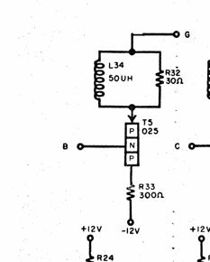
Notice above the that T5 collector is connected to -12V through a moderately low resistance (300 ohm) and the emitter is connected directly to the output pin G through a very low DC resistance (30 ohm, we’ll come back to the inductor later).
The key thing to understand here is that for this particular card: when the transistor is “on” it provides a strong path to -12V (logic 0) for anything connected to pin G, and when the transistor is “off” pin G is essentially floating at high impedance - it’s almost like the pin is disconnected.
Contrast that with the output stage of many of the other logic cards. TAG - 2-input NAND is a very common example and is used heavily in the 1620:
It’s a bit confusing because the transistors are drawn upside down, but you can see in the picture above that the emitter is connected to ground and the output is taken from the collector. When the transistor is on pin G it is strongly tied somewhere close to ground (logic 1) and when the transistor is off pin G is weakly tied to -12V (logic 0) through R32 circled in red.
Important take-away: the CEYB card provides an ambiguous logical output when the transistor is off, whereas the TAG card provides an unambiguous output in all cases.
Given how many CEYB cards are used in the 1620 there must be something else going on.
The key is to recognize that SMS cards often work in concert with one another. This is a tricky nuance and is hard to get used to for someone used to dealing with Lego-like logic families such as 74xx and 40xx. This is a good reminder that it’s all analog at the end of the day! (Side note: not sure how we’re going to deal with this in Verilog yet.)
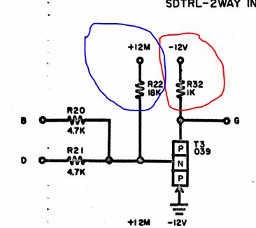
If we look at the input of the card that is being driven by the CEYB output in the example above (TFC - compensated low power inverter in this case) we see that the input pin P is being held up to +12V via R23 (circled in blue) in the case that P isn’t otherwise connected.

So the “ambiguous” state on the CEYB.G output when it’s driver transistor is off is resolved by the R23 pull-up on the input stage of TFC.P, assuming these cards are connected to each other. In that case, the CEYB.G becomes unambiguously logic 1 with a little help from its TFC friend. See the path highlighted in blue:
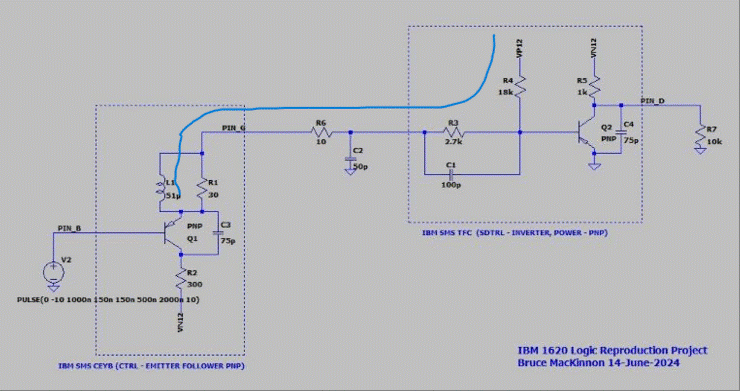
This is important and still fully relevant in modern times so it makes sense to setup the situation in SPICE for more analysis. For starters, assume a one-to-one connection (i.e. one output tied to one input). Disregard the RC circuit between the two cards - that is for modeling a longer inter-card connection wire. Likewise, the CE capacitors are placeholders for parasitic effects to be modeled later.
The SPICE simulation trace looks like this:
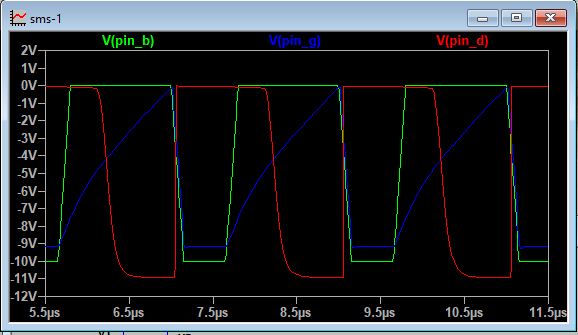
Key things to observe:
- The green trace is the driving input of the CEYB card on the far left.
- The blue trace is the output of the CEYB card. As expected, it follows the CEYB input within one junction drop. It’s an emitter follower.
- The red trace is the output of the TFC card. It is a logical inversion of the blue input, as expected.
Everything is working.
IMPORTANT: The default PNP transistor models in NGSPICE are based on modern silicon devices. I’ve been using a SPICE transistor model file that more closely simulates a germanium transistor, but this is far from accurate at this time. In particular, the early transistors used in the 1620 undoubtedly had some relatively huge parasitic capacitances that impacted performance. I’ve not tackled this problem yet so many of the simulations present an unrealistically “sharp” view of the analog waveforms. I will do some work on this facet of the model later.
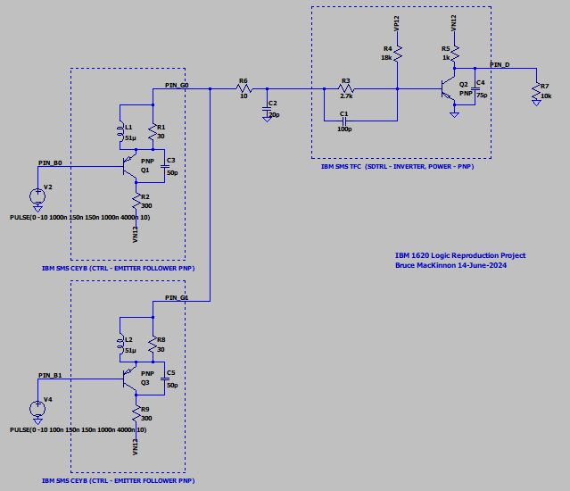
Now for the important case. Assume that the output of two CEYB cards are tied together and are both connected to the TFC card input:
Here is the output of the SPICE simulation:
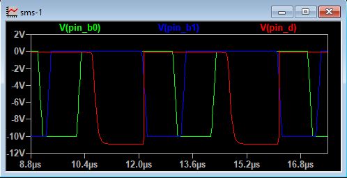
Key things to observe:
- The green and blue traces are the inputs of the two CEYB cards on the far left. They have been intentionally delayed in phase.
- The red trace is the output of the TFC card, as before. Note that the TFC output is a logical 1 whenever either of the two CEYB inputs is a logical 0. You can think of this as a NOT-OR function.
Here we can see that both of the CEYB cards have the equal ability to pull the input of the TFC card down to logical 0, regardless of what the other CEYB card is doing. Even though the cards have their outputs connected, there is no logical conflict. We get a free OR gate out of the deal, which is one of the reasons that the cards are designed this way.
Recalling the error checks that IBM built into their “Design Mechanization System,” compatibility between SMS cards was one of the things that the system was looking at automatically. We’ll only get the desired OR behavior with cards that are designed to work like this.
A last note on terminology. Above it seemed like TFC was reacting to a logical 0 of either one CEYB OR the other. But the comment in the ALD says “DOT AND.” I’m assuming this terminology refers to the fact that the dot on the ALD diagram that connects the multiple outputs is performing a logical AND operation.
In fact, this statement appears in the 1959 IBM Transistor Components Circuit manual:
DOT Functions
Under certain conditions, outputs of similar levels can be tied together, to share a common load. This connection provides a second level of logic in the output circuits, and is referred to as a DOT function …
The confusion between AND dot and OR dot is probably related to the fact that a NAND can be re-written as a NOT-OR, per De Morgan. So in our example, if the top CEYB card is a logical 1 AND the bottom CEYB card is a logical 1 then the output of the TFC card is a logical 0. This is a NAND function.
A Note About Verilog
Verilog is for digital simulation. It doesn’t know anything about pull-up resistors on input stages, emitter followers, open collectors, etc. Those are all realities of circuit design in a more complicated analog world. In order to properly simulate circuits that make use of SMS dot-OR/dot-AND constructs our “synthesizer” will need to be smart enough to recognize when multiple output pins are tied to the same wire and insert the appropriate Verilog Boolean expression to realize the digital representation of the analog hook-up. I think this is doable, but we’ll find out.