IBM 1620 - Clock Sequence Notes
A quick post today to document some recent activity.
The Customer Engineering Reference Manual has this diagram in the Condensed Logic chapter on page 19:
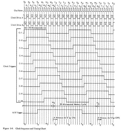
This is a very important diagram because it defines the mechanics of the clocking mechanism used in the 1620. I talked about the master oscillator in an earlier post, but there is more to the story.
The master clock runs at about 1 MHz, so the machine “ticks” ever 1 microsecond. However, this 1 MHz master clock drives a 20 cycle sequence of events that defines one “memory cycle” of the computer. You can think of this 20 microsecond sequence as the fundamental cycle with respect to memory activity: memory is addressed, read from, and written to during the different phases of this 20 microsecond period.
The 20 individual “ticks” inside of the memory cycle are named T0, T1, T2, T3, T4, T5, R0, R1, R2, R3, R4, R5, R6, W0, W1, W2, W3, W4, W5, W6 and each has a specific purpose.
As you can see from the timing diagram, the machine goes through an “advance” process on each W6 tick.
This memory cycle is further segmented into the A and B cycles which are used to initiate alternating memory accesses.
The logic to handle all of this spans pages 01.10.05.1 through 01.10.12.1 of the ALD. Believe it or not, 43 SMS cards must be plugged into the imaginary machine that we are building to make this work. There are 12 different SMS card types used, all of which have been modeled using Verilog now.
Here’s the output of the simulation to show that the results are equivalent to what is shown in the 1962 CE manual. This is an important milestone:
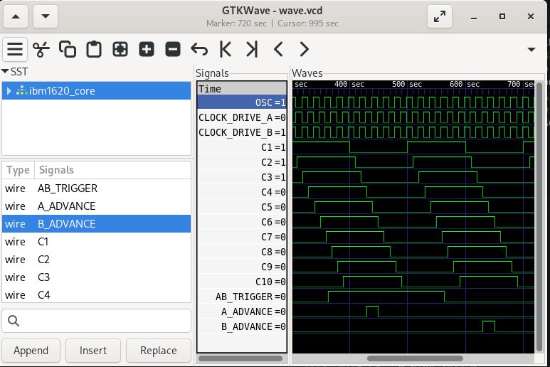
(NOTE: You can disregard the timescale at the top of this diagram.)